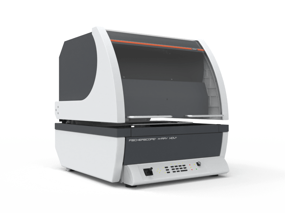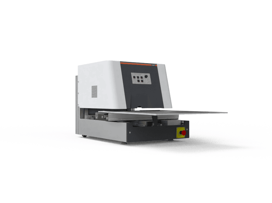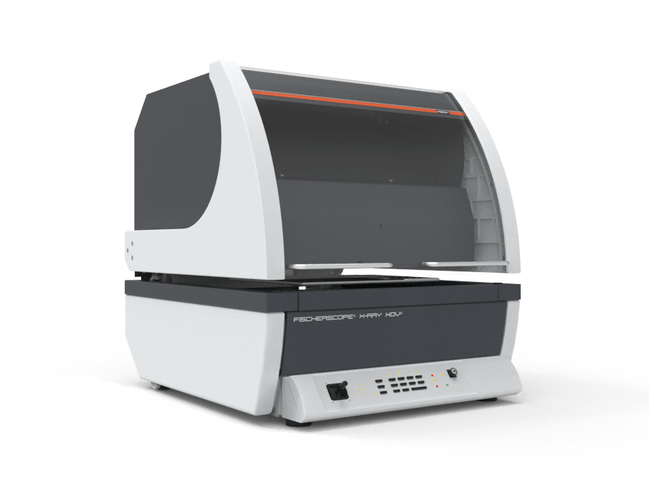
FISCHERSCOPE X-RAY XDV-µ
Smallest measuring spot, highest precision: for very small, flat components and multilayer systems.
Learn more
X-ray system for fully automated measurement of microstructures on wafers up to 12 inches.
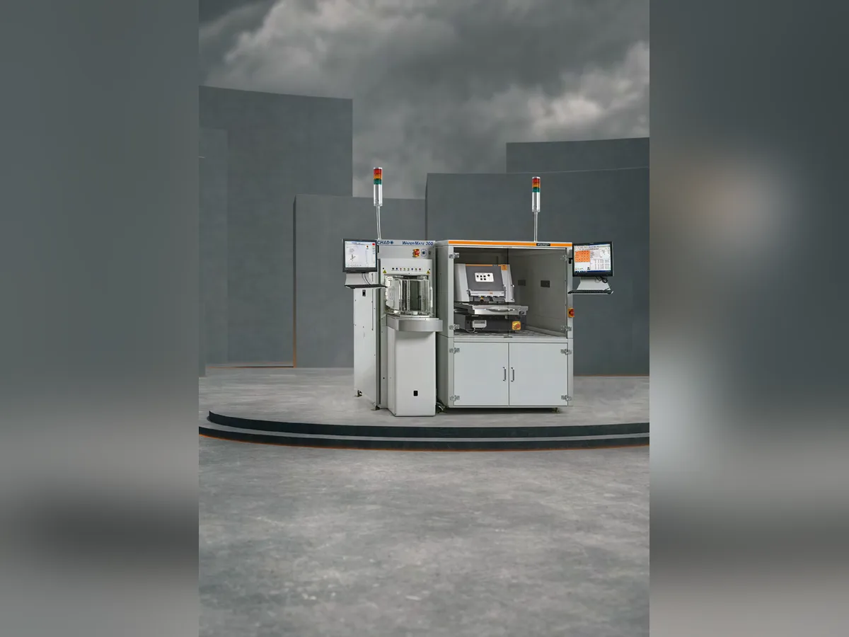
The XDV-µ SEMI is the optimal solution for fully automated inspection of microstructures on wafers. It is suitable for thickness measurement and element analysis of base metallizations in the nanometer range, C4 solder balls, lead-free solder caps on copper pillars, small contact areas and 2.5D/3D packaging. It complies with the relevant SEMI standards and is ideal for process monitoring in manufacturing.
Smallest measuring spot, highest precision: for very small, flat components and multilayer systems.
Learn moreSmallest measuring spot at the largest measuring distance: for measuring the smallest components.
Learn moreThe professional series for PCBs: reliable, fully automatic measurement of the smallest structures.
Learn moreSend an enquiry and we will respond with a tailored quotation or advice.